Equipment
There are five types of products.
- Advanced Packaging Measurement equipment—CFM1, CWS1, HDM1, FM1, TM1
- Advanced packaging comprehensive measuring equipment – ACM1
- White light interferometer series—WLI Series
- Thickness measurement module – nXV
- Optical Triangulation 3D Module – NL
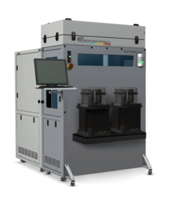
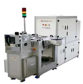
Advanced Packaging Measurement Equipment
CFM1 – CMP Flatness Measurement Equipment
CWS1 – Die Warpage Measuring Equipment
HDM1 – HCB Dishing Metrology Equipment
FM1 – Wafer Warpage Measurement Equipment
TM1 – TSV Metrology Equipment
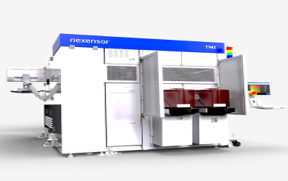
System Overview:
Our advanced measurement system is equipped with high-resolution optics, enabling precise topographic analysis of μ-bumps and microstructures. When wide-area measurements are required, a robust algorithm ensures optimal data accuracy and consistency.
Key Capabilities:
μ-Bump Height Measurement
High-Resolution HBM Warpage & Stress Analysis
Engineered for reliability and precision, supporting advanced packaging inspection needs across diverse applications.
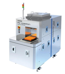
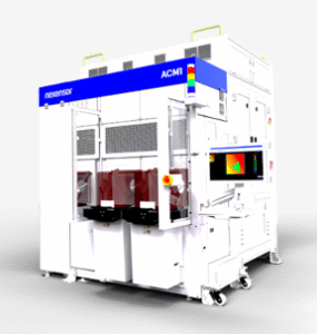
Advanced Packaging Comprehensive Measuring Equipment

CM1 – RDL/CD Metrology Equipment
Overview:
As advanced packaging technologies evolve, the demand for high-precision measurement continues to grow. Leveraging proprietary optical expertise and innovative engineering, the ACM1 enables accurate measurement of key parameters critical to advanced packaging processes.
Capabilities:
Critical Dimension (CD)
Redistribution Layer (RDL) Thickness and Width
Total Indicator Reading (TIR)
Height
Overlay
Compared to conventional measurement systems, ACM1 offers significantly expanded functionality for more comprehensive and detailed process evaluations. Its versatility and precision make it essential for optimizing yield and quality in next-generation packaging lines.
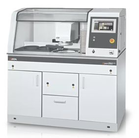
White Light Interferometer Series
- WLI Series – White Light Interferometer
Overview:
Ultra-Precision Measurement Based on WLI Technology. The WLI-based system delivers ultra-precise metrology with high speed and reliability, suitable for mass production environments.
Applications:
Step height, film thickness, and surface roughness at sub-micron levels
Semiconductor microstructures
Bump profiles
Surface defects
Particle-induced protrusions
Other fine features
Key Features:
Fast Measurement: Less than 1 second per scan
Versatile Capabilities: Step height, depth, and roughness
Ultra-Fine Z-Axis Resolution: Down to several hundred nanometers
PSI Mode: Nanometer-level precision
Membrane Separation Function: Layered/membrane-based structure analysis
Auto Focus: Enhances ease of use and repeatability
Proven Reliability: Applied across diverse industries and product lines
This system combines speed, precision, and flexibility to meet next-gen semiconductor and microelectronics demands.
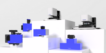
Thickness Measurement Module
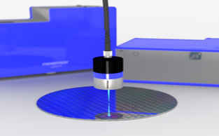
Product:
nXV-1 – Spectral Interference Displacement Laser Sensor
Overview:
An advanced thickness measurement system designed for both transparent (films, glass) and opaque/rough materials (silicon, sapphire wafers). It also measures applications that were previously difficult to evaluate, including secondary battery sealing thickness and PCB conformal coating thickness.
Key Features:
Multi-Channel Support: Up to 16 probe channels on one controller for simultaneous multi-point measurements.
High-Speed Measurement: Optimized for mass production throughput.
Nano-Level Repeatability: Exceptional precision and consistency at nanometer scale.
Multi-Layer Compatibility: Supports diverse material layers across different production needs.
Optical Triangulation 3D Module
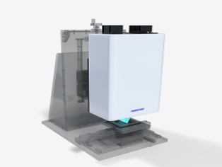
Product:
NL-1 – Optical Triangulation Measurement Module
Overview:
High-speed 3D measurement solution at a competitive price, designed for glossy surfaces and varying height levels, ideal for mass production.
Key Features:
3D Measurement on Glossy Surfaces: Accurate surface profiles even on reflective materials.
Fast & Precise Height Measurement: Multiple height levels, including wafer protrusion height.
Robust & Reliable: High shock resistance for stable performance in demanding environments.
Versatile Application: Suited for industrial fields requiring precision surface and structural analysis.
This system combines affordability with advanced functionality — an excellent solution for high-throughput, precision-driven manufacturing environments.
EQUIPMENT LIST
1.3D wafer Bump & Wire Bonding AOI Inspection System, Wafer Bump 3D Vision Inspection
2. Abatement Systems, Liquid Delivery System
3. Advanced Packaging Measurement equipment, White Light interferometer series, Thickness measurement module, optical triangulation 3D module
4. AI Vision Inspection, Ultrasonic ACF Bonding, Package AI Vision Inspection, Conformal Coating Inspection, LED Vision System, Wafer Vision Inspection, Curved 3D Glass Inspection and measurement, Ultrasonic ACF Bonding
5. AI, AOI, Laser, IR Solution
6. Application: STI, Poly, Contact and Gate Etch, Metal and via/Trench Etch/Cu CMP, Micro ADI/Photo cell monitor, Tool Monitor, Films, and Post-CMP Films/Wafer Inspection System
7. Argon Fluoride Immersion Lithography/ArF: Argon Fluoride Dry Lithography/KrF: Krypton Fluoride Lithography
8. Atomic Layer Deposition, Epitaxy/Silicon Carbide, PECVD, and vertical Furnaces (LPCVD: Low Pressure Chemical Vapor Deposition)
9. ATM System / VTM System / Robots / 300 mm Ion Implanter, Vacuum Robot for High Vacuum Process
- Auto Pressure Controller, Vacuum Transfer System, Dispenser, Refurbished equipment
11. Automation, Ozone System, HORIBA Concentration Monitor, AION PVA Brush
12. Automated Test Equipment, Component Test Systems, Metrology/SEM
13. Ball placement system, camera module system, laser application system, process automation system, Package EMI shielding system, Package sorter P&P system
14. Battery and Semiconductor Inspection
15. Burn-In Sorter/Test Handler, Vision Inspection, Gantry Automation
16. Burn-in Tester and Burn-in Board / MFT, MBT, TBT, MLCC, LBT, and Board
17. Camera Module and Test Equipment (Probe Card), Semiconductor Parameter Analyzer
18. CCSS (Central Chemical Supply System) Wet System, Inkjet printing system
19. Chemical Mechanical Polishing, Wet Cleaning System
20. Clean, Etch, Photo, Test and Package/Line Automation, Transportation, Storage
21. Cube Prober (HBM), Memory Test Handler, SoC Test Handler, Module Test Handler, Test and Vision Solution
22. Descum equipment, descum and surface treatment for wafer-level semiconductor packaging process
23. Deposit metal materials (ITO, Al, Mo, Ag, Ti, IGZO with application), Horizontal Pass with vacuum robot, Industrial deposition
24. Deposition Process Equipment, Treatment (Film Property Improvement Process Equipment), Ultrasonic Generators, Measuring Systems
25. Dicing Saw, Saw & Sorter, MLCC Cutter, Breaker, Tape Mounter, Wafer Cleaner, Mask manufacturing equipment
26.Dispenser, Attach, Laser assisted bonder, Micro SBM, Cu pin, Laser compression bonder, Protec laser reflow, Bin sorter
27. Dry Etcher for Mobile Display, EV/Glass Treatment/Organic, Metal Deposition Process/Bio Health, Medical and Cosmetic
28. Dry Strip, Dry Cleaning, NHM Strip, Edge Clean
29. Edge Grinder, Edge Profiler, Drilling Machine, Cover Glass Grinder, Mother Glass Grinder/Machining, Inspection and Laser Total Solution, Surgical Robot, Sensors
30. Etchers and nano implant / ICP Etcher, DRIE Etcher, CCP Etcher, LED Etcher, Nano Imprint
31. Etching, Cleaning, Treatment/Automation + Plasma + Vacuum Process
32. EUV lithography solutions
33. EUV Mask Solution, Laser Cleaner, CO₂ Cleaner
34. Exhaust Management, Thermal management
35. FPD repair equipment / Inspection & Analysis
36. Front-End/PE-CVD, ALD, Back-End/Die Bonder, Flip Chip Bonder, TC Bonder, Hybrid Bonder
37. FSH Microscopy Module, FSH AOI (Advanced Packaging), FSH Interferometry Module, FSH Camera Module, Larger area inspection for wafers
38. Gas Supply System, Chemical Supply System
39. Global Smart Factory & Solution, Semiconductor, Display, Second Battery, MH/OHT, Clean Conveyor system, AGV, OHS, Roll OHT
40. HBM TC Bonder, Vision Placement, Micro Saw, EMI Shield, Metal grinder, Laser Ablation and Laser mark
41. High-pressure hydrogen annealing equipment
42. In-Line System, Process Equipment (3D Lamination, Dispenser, Grinder, Bake Oven, Furnace Oven, Micro LED Dispenser)
43. Inspection & Measuring equipment
44. Inspection Automation Equipment (Cap Exterior Inspection, Contamination Inspection, Liquid Level Inspection, Leak Inspection)
45. Jusung Engineering’s ALD equipment achieves uniform and high-quality thin films at temperatures below 300°C, regardless of complex underlying structures, across processes such as ultra-fine DRAM, 200+ layer 3D NAND, and sub-10 nm logic devices
46. Laser solution
47. Manufacturing Stage/Gantry, Air Bearing, Hybrid
48. Memory Tester, SSD Tester, SoC Tester, Burn-in Tester
49. Micro Power Dry System, Native Oxide Removal System, Diffusion Furnace, Vacuum Melting Furnace, Integrated System, Sputtering System, PE-CVD System, Evaporation System, Aching System, Dry Etching System, Ion Implantation System, Vacuum Furnace, Lyophilized
50. Nano Inspection for inner and outer defects of Si Wafer or Glass Substrate, Overlay, Vacuum Stage
51. N2 Purge System, EFEM Dehumidification
52. OHT System, Wire Bonder (Back End), Die Attach (Back End), FOUB Stocker (Back End), Memory Test Handler, EFEM, SMIF (Mask Loader), Try Stocker
53. POU Abatement System, RTO (Regenerative Thermal Oxidizer), IES (Ion Exchange System)
54. Poly Etcher System (Conductor Etcher System), Metal Etcher System, Oxide Etcher System (Dielectric Etcher System)
55. Probe Card, Interface Board, Test Socket, MEMS Product
56. Probe Card, Probe Station, Battery Recycling
57. Quartz, Tungsten, Molybdenum / tube, Bath, carrier, chamber
58. Refurbishing Equipment / CVD Equipment (P-5000, Centura-5200, Ultima-HDP, Producer, 300 mm Producer-SE/GT, 300 mm Ultima-X), PVD Equipment (Centura PVD, Endura-5500, 300 mm Endura-CL/II), Etch Equipment (Centaur DPS + Metal, Centaur DPS + Poly, Centura Super E/eMax), RTP Equipment (Centura XE+/DPN), EPI Equipment (Centura EPI)
59. Scrubber and Chiller
60. Semiconductor: DI, ABF Via Drilling, TGV (Through Glass Via) / Display: Laser cutters for Display
61. Semiconductor Equipment (VACTRA, ATRA, Vacuum Transfer Solution and ATM Transfer Solution)
62. Semiconductor, Display, EV Battery, and Solar Cell Industry / Semiconductor: Rapid Thermal Process, Sputter System, Descum System, Laser Dicing, Laser Annealing, and Laser Ablation. EV Battery: NG Sorter, Tray Washer, Cell Tapping, and Packing. Solar Cell: LEI, LDSE, LCO
63. Semiconductor Manufacturing Equipment (THC, Dehumidifier, CHR)
64. SIC Epitaxy for power semiconductor, Wide Process Hard Mask
65. Solder Ball Attach, Marking System, Package Laser Saw System, Router System, Flux Pre-Cleaning System, Solder Ball Attach Tool kit
66. Standard WTR, Telescopic WTR, SCARA Robot, Cartesian WTR, LED Wafer Transfer Robot, Glass Wafer Transfer Robot, FOUP Handling Robot, and Vacuum Robot. Modules: FOUP Opener, Cassette Loader and EFFM (Equipment Front End Module)/Dental Machine
67. Strip Marker (2 Beam / 4 Beam marker), Tray Marker, Wafer topside and backside marker, Wafer ID marker, Grooving & Dicing, PKG Cutting, Pop drilling
68. Sputtering System (Loader System, Roll-to-Roll system (Flexible Substrate), Vertical Cluster Sputter, In-Line Horizontal Sputter)
69. Temporary Wafer Bonding System, Wafer De-Bonding System, Collective Die to wafer Bonding system, Vacuum Cluster System, EFEM, Wafer Transfer Robot, Load Port Module, Pre-Aligner
70. The front-end process (Clean, Etch, strip), the back-end process (Flux, Etch, debond), memory and logic devices, rapid heat treatment for silicon wafers
71. Thermal LPCVD, Plasma Treatment, Large Batch Thermal ALD System, Mini Batch and Dry Cleaning
72. Thin Film deposition system
73. Tools of wet processing, Electrochemical Plating, thermal deposition processing, Track Systems, PECVD, Stress-Free Polishing
74. Transfer Module (Aries Series) / PM (GAS, CDA, PCW : Process Cooling Water)
75. Wafer Macro Inspection, Wafer Review Station, Wafer Warpage Inspection, Wafer Edge Macro Inspection, Mount Inspector, Die Attach Inspection, Wire Bonding Inspection, Stocker System (ASRS), Tower Lifter and rail